From Circuitcaster to a PCB in your mailbox.
Circuitcaster is the friendly front — schematics, footprints, board layout on a touch grid. KiCad is the industrial back — routing, DRC, Gerber generation, fab-ready output. This page shows you the full pipeline end-to-end using the FleetCom Node project as a running case study — a real 2-board audio device that went from Circuitcaster idea to physical PCBs from JLCPCB.
circuitcaster.com/kicad-export/for-ai.txt — install commands per OS, complete conversion script, verification steps, success criteria. The Python script itself is at circuitcaster.com/kicad-export/cc_to_kicad.py. Grab both, tell the user which tools to install, run the script against their export, walk them through the human-only steps (schematic authoring + 1:1 print verify) that follow.
curl -O https://circuitcaster.com/api/watch/<workspace-id>/kicad.zip.kicad_pro → schematic + PCB are both there, ready to route + Gerber. The steps 3-5 in the pipeline below (footprint conversion, symbol authoring, schematic wiring) collapse into that one HTTP call. Steps 6-9 (route, DRC, Gerbers, order) remain the human/KiCad side of the workflow.
What's in the zip:
.kicad_pro (project), .kicad_sch (schematic with embedded symbol library, placed components, wires between pins, and global labels for VCC / GND), .kicad_pcb (PCB with placed footprints, board outline, mounting holes, and named nets on every pad), .pretty/ footprint library, fp-lib-table, and a README.md with next-step instructions.
Auth model: Public — the workspace id is the share secret (128-bit random, unguessable). Authenticated variant at
GET /api/v1/workspaces/<id>/kicad.zip for private workspaces (requires a cc_... API key generated at /account/api-keys).
Overview.The 9-stage pipeline
dotgame.project_bundle.v1 JSON..kicad_mod file.1.Install KiCad
Download KiCad 8 or newer from kicad.org/download. The FleetCom case study uses KiCad 10.0.3 (latest at time of writing). KiCad 8 works too; any earlier version is missing the schematic editor polish you'll want.
- Windows: Grab the .msi installer. ~1 GB. Runs on Windows 10 or newer.
- macOS: .dmg with universal binary. Runs on macOS 12+ (Intel and Apple Silicon).
- Linux: Available in most distro repos (
apt install kicad) or as an AppImage from the site.
After install, KiCad shows a "Project Manager" — this is your home base. Everything (schematic, PCB, footprints, libraries) is organized inside project folders.
2.Export from Circuitcaster
In app.circuitcaster.com, open the project you want to fab. Tap Send in the top-right corner. The app writes a dotgame.project_bundle.v1 JSON — this is the fab handoff artifact and carries everything downstream needs:
- Every component with its footprint reference, position, rotation
- Every wire with its from/to pads, layer, and bends
- Board outline (rect or circle), mounting holes, corner radius
- Pre-computed nets — every pad grouped by electrical connectivity
- The full footprint library — pad geometry, board size, pitch, per-pad names/roles
- An embedded
_ai_briefingand_ai_edit_instructionsso any AI can consume it without external context
The schema is documented at app.circuitcaster.com/llms.txt under "Project bundle schema."
3.Convert JSON to KiCad footprints
Each unique component type in the export becomes one .kicad_mod footprint file. Circuitcaster's pad geometry is already in KiCad's coordinate convention (X right, Y down, origin at component center) so the conversion is direct.
Minimal Python recipe — takes one footprints[] entry and writes a .kicad_mod file:
def cc_to_kicad_mod(fp_name, cc_footprint):
    """cc_footprint is one entry from project_bundle.footprints{}.
    Returns a KiCad 6+ .kicad_mod S-expression string."""
    pins = cc_footprint["pins"]  # each has n, kicad_xy_mm[x,y], role, name
    w, h = cc_footprint["board_mm"]["w"], cc_footprint["board_mm"]["h"]
    lines = [f'(footprint "{fp_name}"',
             f'  (version 20240108)(generator "circuitcaster")',
             f'  (layer "F.Cu")(attr through_hole)']
    # board outline on Edge.Cuts
    hw, hh = w/2, h/2
    for a, b in [((-hw,-hh),(hw,-hh)), ((hw,-hh),(hw,hh)),
                 ((hw,hh),(-hw,hh)),  ((-hw,hh),(-hw,-hh))]:
        lines.append(f'  (fp_line (start {a[0]} {a[1]}) (end {b[0]} {b[1]})'
                     f' (stroke (width 0.12) (type solid)) (layer "Edge.Cuts"))')
    # pads: through-hole, 1.6mm annular, 0.8mm drill. Adjust to your part.
    for p in sorted(pins, key=lambda p: p["n"]):
        x, y = p["kicad_xy_mm"]
        shape = "rect" if p["n"] == 1 else "circle"  # rectangle marks pin 1
        lines.append(f'  (pad "{p["n"]}" thru_hole {shape}'
                     f' (at {x} {y}) (size 1.6 1.6) (drill 0.8)'
                     f' (layers "*.Cu" "*.Mask"))')
    lines.append(')')
    return "\n".join(lines)
Save output as <fp_name>.kicad_mod in your project's lib/<yourproj>.pretty/ folder. Register the folder in fp-lib-table so the PCB editor sees it.
4.Author symbols + wire the schematic
KiCad separates schematic symbols (electrical shape) from PCB footprints (physical pads). Circuitcaster's exported JSON is footprint-first (that's the touch design), so you author a schematic symbol per component in KiCad's Symbol Editor, then wire them in the Schematic Editor.
Fast track: label-based wiring. Instead of drawing wires everywhere, drop hierarchical labels (e.g. DAC_BCK, MIC_SD, +3V3) on the pins that share a net. KiCad treats identical labels as a single net. Result: a clean schematic with visual nets grouped by signal, not tangled by geometry.
Add PWR_FLAG markers to each power net (once for +3V3, once for GND) so ERC knows a power source exists.
5.Update PCB from Schematic
From the Schematic Editor, hit F8 or Tools → Update PCB from Schematic. KiCad reads the netlist, matches every schematic symbol to its footprint by Reference, and places footprints on the PCB with a "ratsnest" — thin lines showing every unrouted electrical connection.
You're now in the PCB Editor. Move components around to minimize crossings. Set the board outline (Edge.Cuts layer) to whatever size your enclosure demands.
6.Route the traces
Two options:
- Freerouting (autorouter, recommended for first pass): KiCad exports a Specctra DSN file, you feed it to Freerouting, it produces a Specctra SES file, you import it back. 2-minute round-trip for a small board.
- Manual routing: Click each rat-line to draw the trace by hand. Tedious but you control everything. For 2-layer designs with <30 nets it's honestly not that bad.
Either way, drop a ground pour on the bottom copper (Add filled zone → B.Cu → GND) so all your GND pads have a solid return path.
7.DRC — Design Rule Check
Run Inspect → Design Rules Checker. Errors here are things the fab house will reject: clearance violations, unrouted nets, tracks off the board, hole-too-close-to-edge. Fix each one. Warnings can usually be ignored, but skim them.
(no_connect) markers or a KiCad rule exception to silence.
8.Export Gerbers
File → Fabrication Outputs → Gerbers. Enable these layers (standard 2-layer job):
- F.Cu (top copper)
- B.Cu (bottom copper)
- F.Paste, B.Paste (solder paste — only if you're doing SMT assembly)
- F.SilkS, B.SilkS (silkscreen — the white component labels)
- F.Mask, B.Mask (solder mask openings)
- Edge.Cuts (board outline)
Also export drill files: File → Fabrication Outputs → Drill Files. Use the Excellon format, PTH and NPTH in separate files, "Use Protel filename extensions" for JLCPCB compatibility.
Zip the whole Gerber output folder into one .zip. That's your fab handoff.
9.Order from a fab house
Two mainstream options that ship anywhere for a few dollars:
- JLCPCB — cheapest, fast. $2 for 5 boards of a 100×100mm 2-layer design + shipping. Upload the Gerber zip on the front page; site parses it automatically, shows a preview, checks it for common issues. 3-5 days to fab + shipping.
- PCBWay — slightly pricier, better for tricky specs (large boards, flex, rigid-flex, HDI). Also has an active project sharing community.
Both accept the KiCad Gerber zip directly. Neither requires you to know their proprietary format — this is the universal handoff industry has agreed on.
Case study.FleetCom Node
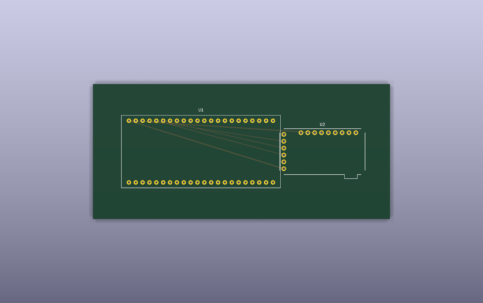
The FleetCom Node is a real audio-mesh device: ESP32-S3 + PCM5102A DAC + 2× INMP441 mics + JST-XH 5-pin cable + WS2812 LED ring. Two physically separate boards, joined by a 6-inch cable. Designed on Circuitcaster, converted through this exact pipeline, ordered from JLCPCB. Here it is.
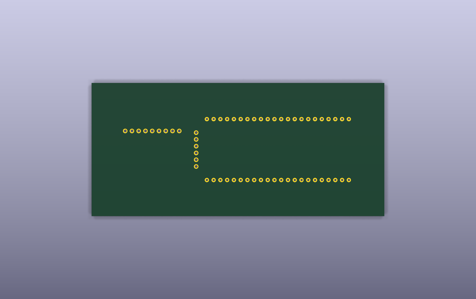
Board 1 — Main board
ESP32-S3 socket, PCM5102A DAC module, 3.5mm audio jack on the DAC module, JST-XH connector to the mic board.
Board 2 — Mic board
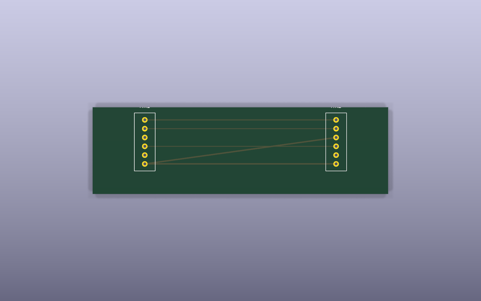
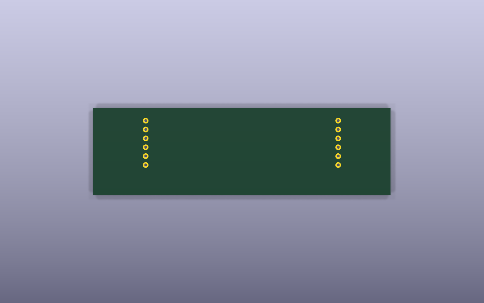
Two INMP441 MEMS microphones at 55 mm baseline (for stereo / beamforming), JST-XH connector to the main board. Same shared SCK/WS bus, one-wire stereo I2S trick — each mic drives SD on its own half of the frame.
Custom footprints authored
Three non-standard modules needed their own .kicad_mod files, all authored from Circuitcaster exports and verified against physical hardware with the 1:1 print check:
| Footprint | Dimensions | Source |
|---|---|---|
| LB_ESP32_S3_44pin | 62.64 × 25.73 mm, 2×22 header, 22.86 mm row pitch | DotGame v0.3.2 (touch-designed) + calipers-verified |
| GY_PCM5102_Module | 20 × 18 mm, 1×6 + 1×5 header | Circuitcaster export → vendor silkscreen photo verify |
| INMP441_Module | 6 × 17 mm, 1×6 single-row | Circuitcaster export → module outline caliper measure |
Gerber output
Two zip files, ready to upload to JLCPCB:
fleetcom_main_board_v0.1_PRELIMINARY.zipfleetcom_mic_board_v0.1_PRELIMINARY.zip
Each contains 8 Gerber layers + 2 drill files + a fab-notes README.
armada/pcb/fleetcom_node/ in the repo. Open the .kicad_pro files with KiCad 8+ and you're inside the whole design in seconds.
Ready to try the pipeline?
Design your circuit on Circuitcaster. Export the JSON. Follow this guide. Order the board.
⚡ Open CircuitcasterQuestions on any step? Email [email protected] — I'll help you unstick it.